Raman Lab
Exploring the frontiers of Quantum Materials and Quantum Transport at TIFR Hyderabad.
"The mind that is open to new ideas never returns to its original size." - Albert Einstein
About Us
We are an experimental condensed matter physics lab. Our work focuses on the fascinating properties of quantum material heterostructures and their applications in quantum transport. We delve into cutting-edge areas such as molecular spintronics and proximity effect studies at hybrid interfaces. Our passion lies in understanding the fundamental principles that govern the quantum world, with an eye toward discovering new phenomena and developing next-generation technologies.
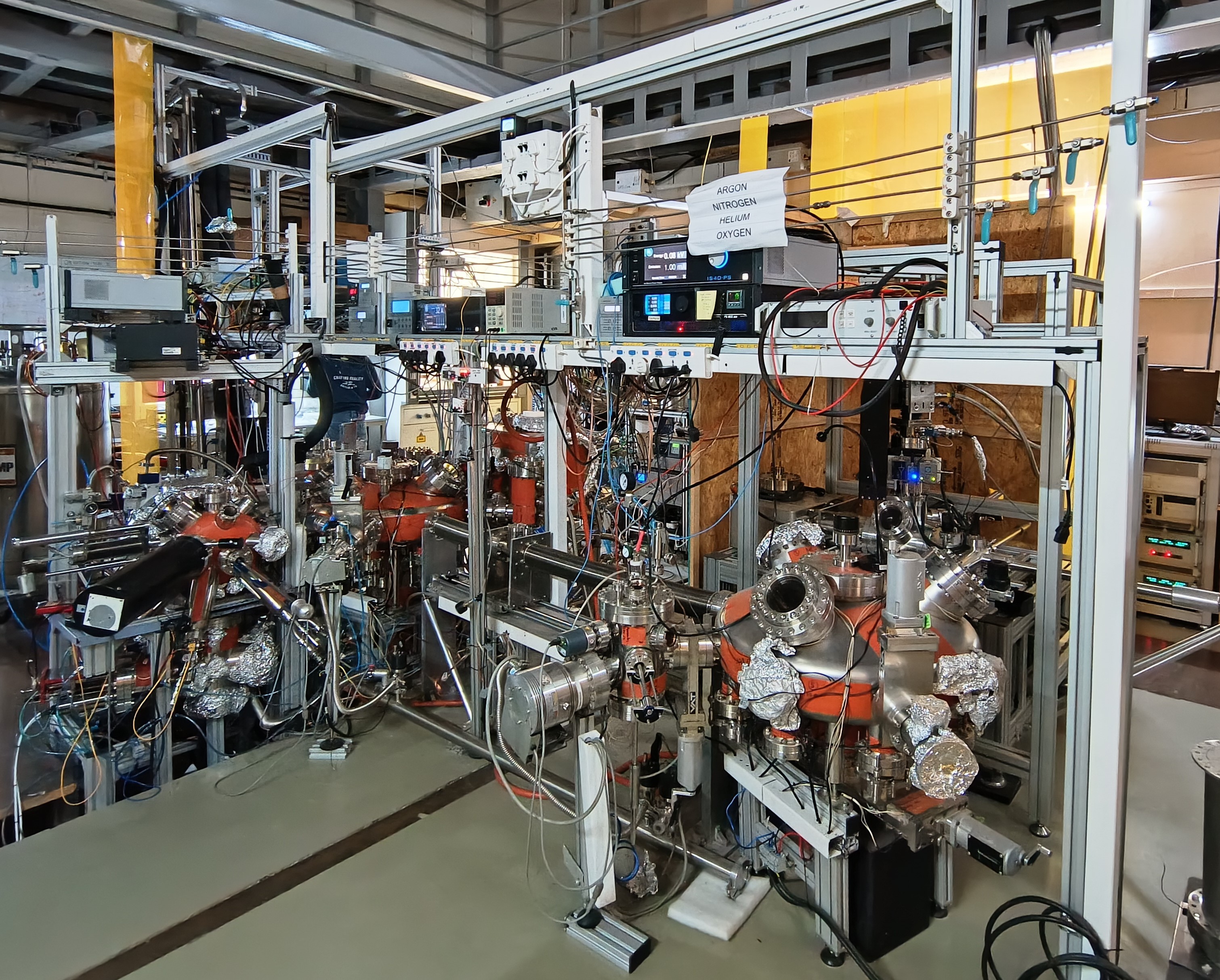
A cornerstone of our research is our ability to design and build our own state-of-the-art Ultra-High Vacuum (UHV) cluster vacuum systems. Our current system is a testament to this, housing advanced capabilities like Molecular Beam Epitaxy (MBE), an 8-target DC/RF sputtering, an oxygen plasma source, an ion milling/heating station, and a Low-Temperature Scanning Tunneling Microscope (LT-STM). This sophisticated setup allows us to precisely fabricate and characterize a wide range of materials, including topological insulators, superconductors, ferromagnetic insulators, and antiferromagnets, enabling us to explore the topological nature of interface states and other intriguing quantum phenomena. Being an instrumentation intensive program, researchers in our group are uniquely trained to become masters in growth.

Research Areas
Interface-assisted Molecular Spintronics
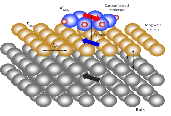
A fascinating field where our group is internationally leading the efforts to explore magnetism and spin control at surfaces of exotic materials using molecular adsorption, paving the way for fundamental understanding of interface physics and advanced electronic devices.
Proximity Effect Studies
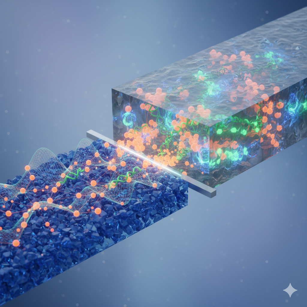
We investigate how novel quantum effects emerge as a consequence of interfacing materials with differential quantum mechanical classification such as topological insulators, ferromagnets, antiferromagnets and superconductors, thereby creating novel hybrid systems.
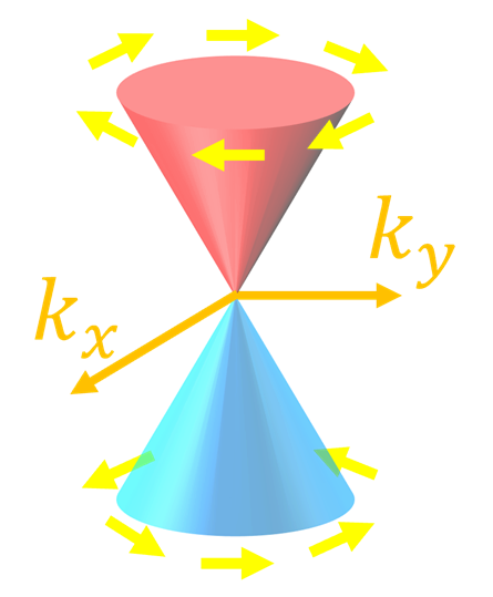
Topological States
Exploring unique, robust quantum states found in materials like topological insulators and superconductors, which are protected from external perturbations.
Publications & Patents
Below are some of our featured publications.
Featured Publications
- Emergence of planar topological Hall anisotropy in Bi2(Se,Te)3 by proximity-induced spin-canted state of the Heisenberg ferromagnetic insulator EuS,Dhavala Suri, Satyaki Sasmal, Archit Bhardwaj, Juhi Singh, Suman Mundlia, Anshika Mishra, Narayan Mohanta, and Karthik V. Raman, Phys. Rev. B 110, 134433, 2024
- Anisotropic planar Hall effects in Bi2Se3/EuS interfaces: Deciphering the role of proximity-induced spin canting and topological spin texture, Juhi Singh, Karthik V. Raman, and Narayan Mohanta,Phys. Rev. B 110, 125133, 2024
- Longitudinal magnetoconductance and the planar Hall conductance in inhomogeneous Weyl semimetals, A Ahmad, KV Raman, S Tewari, G Sharma, Physical Review B 107, 144206, 2023
- Decoupling intranode and internode scattering in Weyl fermions, G Sharma, S. Nandy, K. V Raman and S. Tewari, Physical Review B 107, 115161, 2023.
- Emergence of Unconventional Interfacial Spin Texture in Topological Insulator-Based Magnetic Heterostructures, Dhavala Suri, Archit Bhardwaj, Satyaki Sasmal, Karthik V. Raman, arXiv preprint, 2021
- In-depth Analysis of Anisotropic Magnetoconductance in Bi2Se3 thin films with electron-electron interaction corrections, S Sasmal, J Mukherjee, D Suri, Karthik V Raman, Journal of Physics: Condensed Matter, 33, 46, 2021
- Observation of Planar Hall Effect in Topological Insulator -- Bi2Te3, Archit Bhardwaj, Syam Prasad P., Karthik V Raman, Dhavala Suri, Applied Physics Letters, 118, 241901, 2021
- An all cryogen-free integration of scanning tunneling microscope with superconducting vector magnet in a vacuum cluster assembly with low spectral noise, Saurabh Chaudhary, Janmey Panda, Suman Mundlia, S. Mathimalar, Aathif Ahmedof, and Karthik V. Raman, Review of Scientific Instruments, 92, 023906, 2021
- Sign reversal of anomalous Hall conductivity and magnetoresistance in cubic noncollinear antiferromagnet Mn3Pt thin films, J. Mukherjee, T. S. Suraj, H. Basumatary, K. Sethupathi, and K. V. Raman, Phys. Rev. Materials, 5, 0124201, 2021
- Robust monolayer exchange-bias effect in molecular crane-pulley response at magnetic surface, S. Mundlia*, S. Chaudhary*, L. Peri, A. Bhardwaj, J. J. Panda, S. Sasmal and K. V. Raman, Phys. Rev. Appl., 14, 024095, 2020 (* equal contribution)
- Signature of gate-controlled magnetism and localization effects at Bi2Se3/EuS interface, S. Mathimalar*, S. Sasmal*, A. Bhardwaj, S. Abhaya, R. Pothala, S. Chaudhary, B. Satpati and K. V. Raman, npj Quantum Materials, 5, 64, 2020 (* equal contribution)
- Probing Proximity-Tailored High Spin-Orbit Coupling in 2D Materials, K. R. Sahoo, T. P. Chakravarthy, R. Sharma, S. Bawari, S. Mundlia, S. Sasmal, K. V. Raman, T. N. Narayanan, N. K. Viswanathan, Adv. Quantum Technologies, 2000042, 2020
- Observation of zero bias conductance peak in topologically trivial hybrid superconducting interfaces, S Mohapatra, S Mathimalar, S Chaudhary and K V Raman, Jour. of Phys. Comm., 3, 4, 2019
- “Materials chemistry: A magnetic facelift for non-magnetic metals,” Karthik V. Raman, Jagadeesh S. Moodera. Nature, 524, 42, 2015
- “On the Origin of Steep IV Nonlinearity in Mixed-Ionic-Electronic-Conduction-Based Access Devices,” A. Padilla, G. W Burr, R. S Shenoy, K. V Raman, D. S Bethune, R. M Shelby, C. T Rettner, J. Mohammad, P. Narayanan, A. K. Deb, R. K. Pandey, M. Bajaj, KVRM Murali, B. N. Kurdi & K. Gopalakrishnan. IEEE Transactions on Electron Devices, 62, 963, 2015
- “MIEC (mixed-ionic-electronic-conduction)-based access devices for non-volatile crossbar memory arrays,” R. S Shenoy, G. W Burr, K. Virwani, B. Jackson, A. Padilla, P. Narayanan, C. T Rettner, R. M Shelby, D. S Bethune, K. V Raman, M. BrightSky, E. Joseph, P. M Rice, T. Topuria, A. J Kellock, B. Kurdi & K. Gopalakrishnan. Semicond. Sci. Technol., 29, 104005, 2014
- “Tailoring ferromagnet-molecule interfaces: towards molecular spintronics,” Karthik V. Raman, N. Atodiresei & J. S. Moodera. SPIN, 04, 1440014, 2014
- “Interface-assisted spintronics: Tailoring at the molecular scale,” N. Atodiresei & Karthik V. Raman. MRS Bulletin, 39, 596, 2014
- “Interface-assisted molecular spintronics,” Karthik V. Raman. Appl. Phys. Rev., 1, 031101, 2014
- “Focusing on the molecular scale,” Karthik V. Raman. Nature Nanotech., 8, 886, 2013
- “Interface engineered templates for molecular spin memory devices,” Karthik V. Raman, Alexander M. Kamerbeek, Arup Mukherjee, Nicolae Atodiresei et al. Nature, 493, 509, 2013
- “New method of spin injection into organic semiconductors using spin filtering tunnel barriers,” K. V. Raman, J. Chang, J. S. Moodera. Org. Electronics, 12, 1275, 2011
- “Effect of molecular ordering on spin and charge injection in rubrene,” K. V. Raman, S. M. Watson, J. H. Shim, J. A. Borchers, J. Chang, J. S. Moodera. Phy. Rev. B, 80, 195212, 2009
- “Determining exchange splitting in a magnetic semiconductor by spin-filter tunneling,” TS Santos, JS Moodera, KV Raman, E Negusse, J Holroyd, J Dvorak, M Liberati, YU Idzerda, E Arenholz. Phys. Rev. Lett., 101, 147201, 2008
- “Large spin diffusion length in an amorphous organic semiconductor,” JH Shim, KV Raman, YJ Park, TS Santos, GX Miao, B Satpati, JS Moodera. Phys. Rev. Lett., 100, 226603, 2008
Patents
- Cryogenic Apparatus and An Interconnected Network Thereof for Multi-Core Quantum Processor Architecture, K. V. Raman, D. Suri, A. Ahmedof - Indian Prov. App. No. 202021047505 (2020).
- Low Power thermal imager, Karthik V. Raman & KVRM Murali US Patent No. 20140361397A1 (2015).
- Method of modeling concentration of reducible mobile ionic dopants in semiconductor device simulator, Karthik V. Raman, Mohit Bajaj & Stephen Furkay, US Patent Application No. 20150192533 (2015).
- High density molecular memory storage with read and write capabilities, Karthik V. Raman & J. S. Moodera, WO Patent 8,711,600 (2013).
Collaborations/Services
Collaborations
The Raman Lab is committed to fostering collaborations with leading research groups and institutions, both nationally and internationally. We believe that groundbreaking science often happens at the intersection of diverse expertise.
We are also passionate about scientific outreach and engaging with the broader community to inspire the next generation of scientists.
For collaboration proposals or outreach inquiries, please get in touch with our Principal Investigator via the contact information provided below.
Services
Leveraging our extensive expertise in designing and manufacturing Ultra-high vacuum (UHV) systems, our lab offers consultation services for a variety of research and industrial needs.
We also provide specialized custom coating services, utilizing our advanced magnetron sputtering and MBE systems to deposit high-quality thin films with precise control.
To inquire about our services or request a consultation, please contact us with details of your specific requirements.
Our Team
Principal Investigator
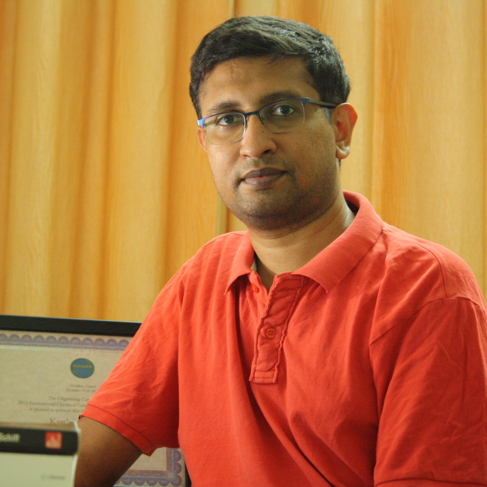
Dr. Karthik V. Raman
Principal Investigator
Current Members
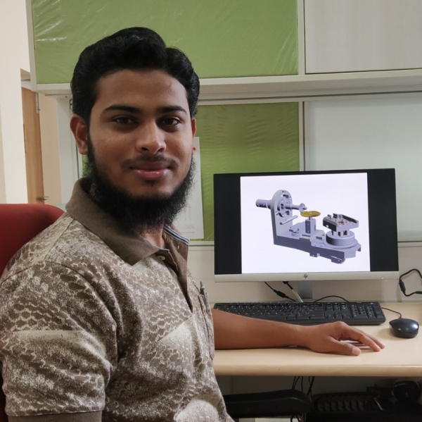
Aathif Ahmedof
Facility Manager
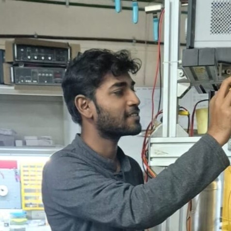
Swapnil Sarjerao Sagare
Scientific Assistant
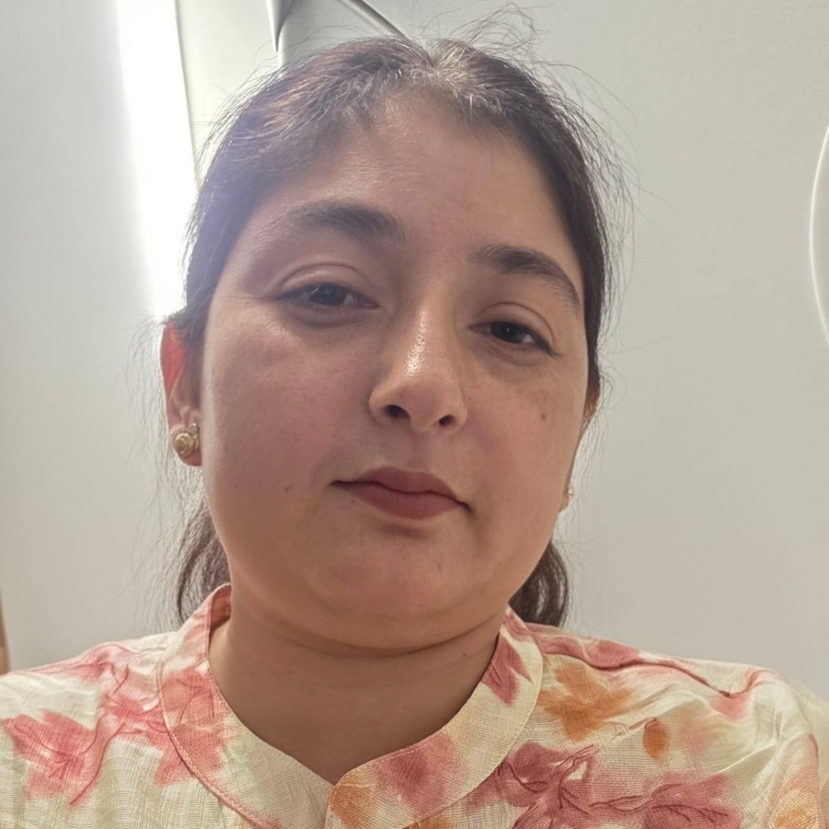
Anshu Verma
Visiting Scientist

Prasad Padhye
Project Scientific Assistant

Malavika Chandrasekhar
Post doctoral fellow

Priyanka Mitra
Post doctoral fellow
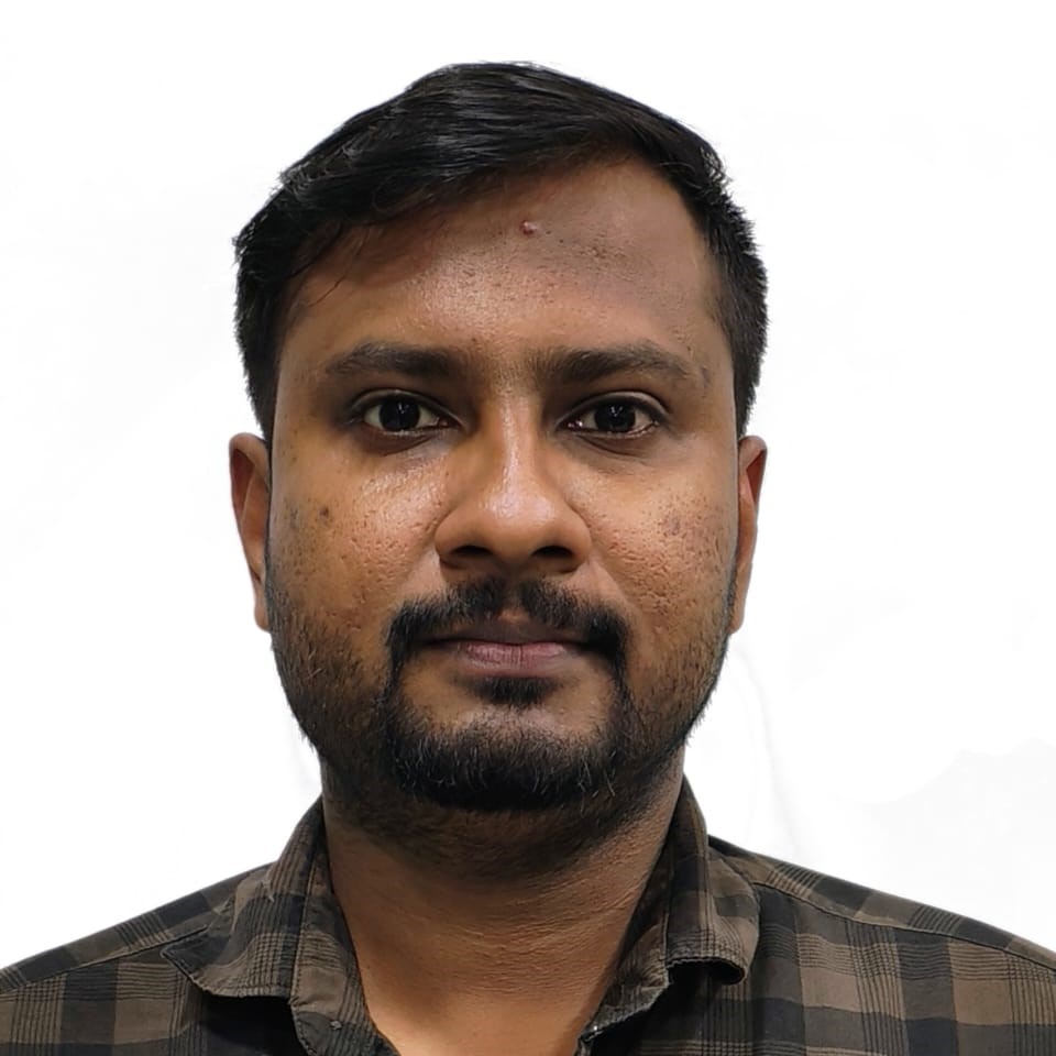
Subhadip Manna
Post doctoral fellow

James Wilson
Project Student
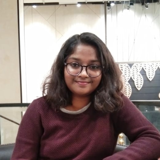
Debalina Giri
Project Student
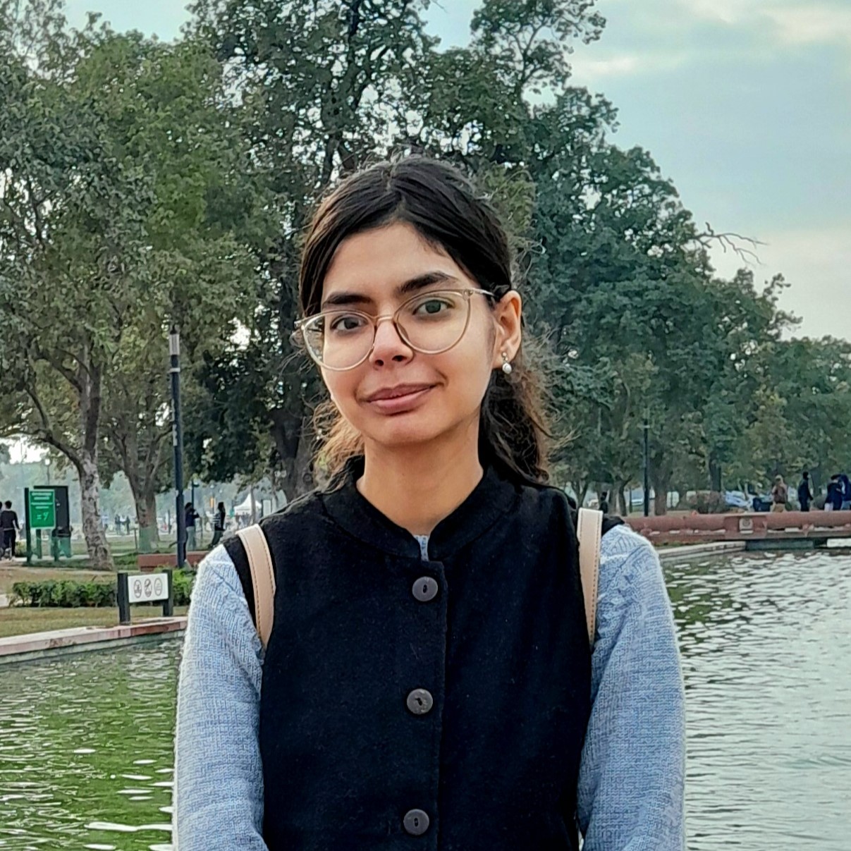
Dhrriti Hira
Project Student
Alumni
-

Ritesh Sachan (Postdoctoral Fellow at TIFRH)
Currently a Post Doc at IIT Kanpur
-
Suman Mundlia (PhD and Postdoc fellow at TIFRH)
Currently a faculty at SRM Institute of Technology, Chennai
-

Bhargava Rajyaguru (Postdoctoral Fellow at TIFRH)
Currently at Uppsala University, Sweden (Postdoctoral fellow)
-
Girija Shankar Papanai(Postdoctoral Fellow at TIFRH)
-

Anjan Bhukta (Post doctoral researcher at TIFRH)
Currently a Senior Postdoctoral fellow at IACS Kolkata
-
Mukil M.(Project Intern Student at TIFRH)
Currently a Ph.D student at MPQ, University Paris Diderot, Paris
-
Satyaki Sasmal (graduate student at TIFRH)
Postdoctoral Fellow at Niels Bohr Institute, Denmark
-
Saurabh Chaudhary (graduate student at TIFRH)
Postdoctoral Fellow at Hong Kong Polytechnic University
-
Dhavala Suri (post doctoral researcher at TIFRH)
Currently a faculty at IISc Bangalore
-

Joynarayan Mukherjee (post doctoral researcher at TIFRH)
Currently faculty (contractual) at IIEST Shibpur, West Bengal
-
Soumya Sankar(SRF at TIFRH)
Currently a Ph.D student at HK University of Science and Technology, Hong Kong
-

S. Mathimalar (post doctoral researcher at TIFRH)
Currently a faculty at SRM institute of Technology
-

Rajasekhar Pothala (post doctoral researcher at TIFRH)
Currently a faculty at NMIMS Shirpur
-

Sambit Mohapatra (SRF at TIFRH)
Currently a Ph.D student at University of Strasbourg, France
-
Swapnil Pathak (SRF at TIFRH)
Currently a Ph.D student at University of Strasbourg, France
-

Anshika Mishra (JRF at TIFRH)
Currently a Ph.D student at Aalto University, Finland
-

Rajesh Kumar (JRF at TIFRH)
Currently a Ph.D student at IIT Hyderabad, India
-
Rita Abani (VSRP at TIFRH)
Currently a Ph.D student at Harvard University
Facilities

In-House Instrumentation
A cornerstone of our research is our custom-built, interconnected Ultra-high vacuum (UHV) cluster system — a key asset that enables our work. This sophisticated setup houses dedicated chambers for thin film growth and in-situ characterization, allowing us to fabricate and study materials with atomic precision.
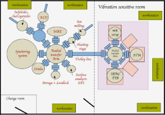
UHV Cluster system
A custom-built interconnected Ultra-high vacuum system for thin film growth and in-situ characterization. This facility, unique in the country, allows in-situ transfer of samples between dedicated growth and characterization UHV chambers.
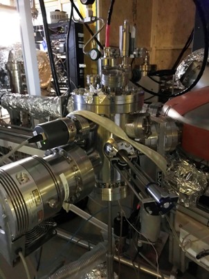
In-situ Oxygen plasma, heating station and Argon ion milling
Dedicated chambers for surface cleaning, controlled oxidation, ion milling for small-area samples, and heating station up to 2000 K for STM surface preparation.
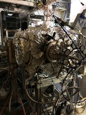
Turret-style DC/RF magnetron sputtering system
The in-house designed 8+2 target DC/RF turret-style sputtering chamber with local gas injection for both inert and reactive sputtering enables wide material growth without cross-contamination.
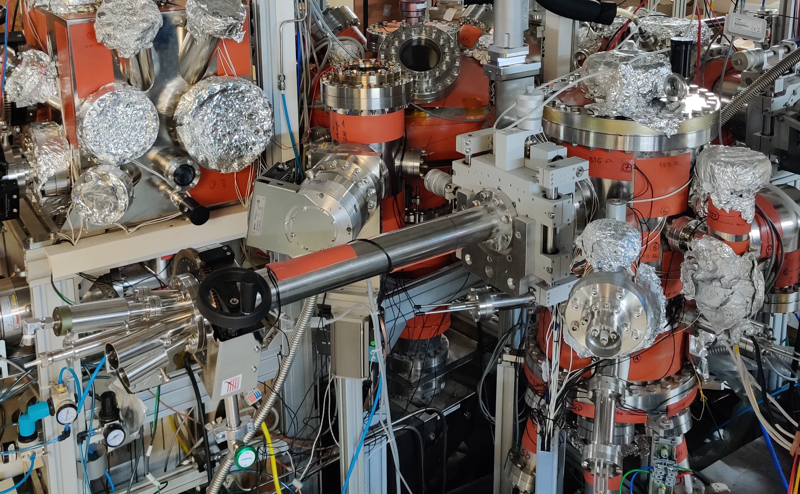
Molecular Beam Epitaxy (MBE) System
The in-house designed MBE system with base pressure of 5×10⁻¹⁰ mbar includes 5 e-guns, 5 Knudsen cells, RHEED, and substrate temperature control from ~100 K to 1700 K.
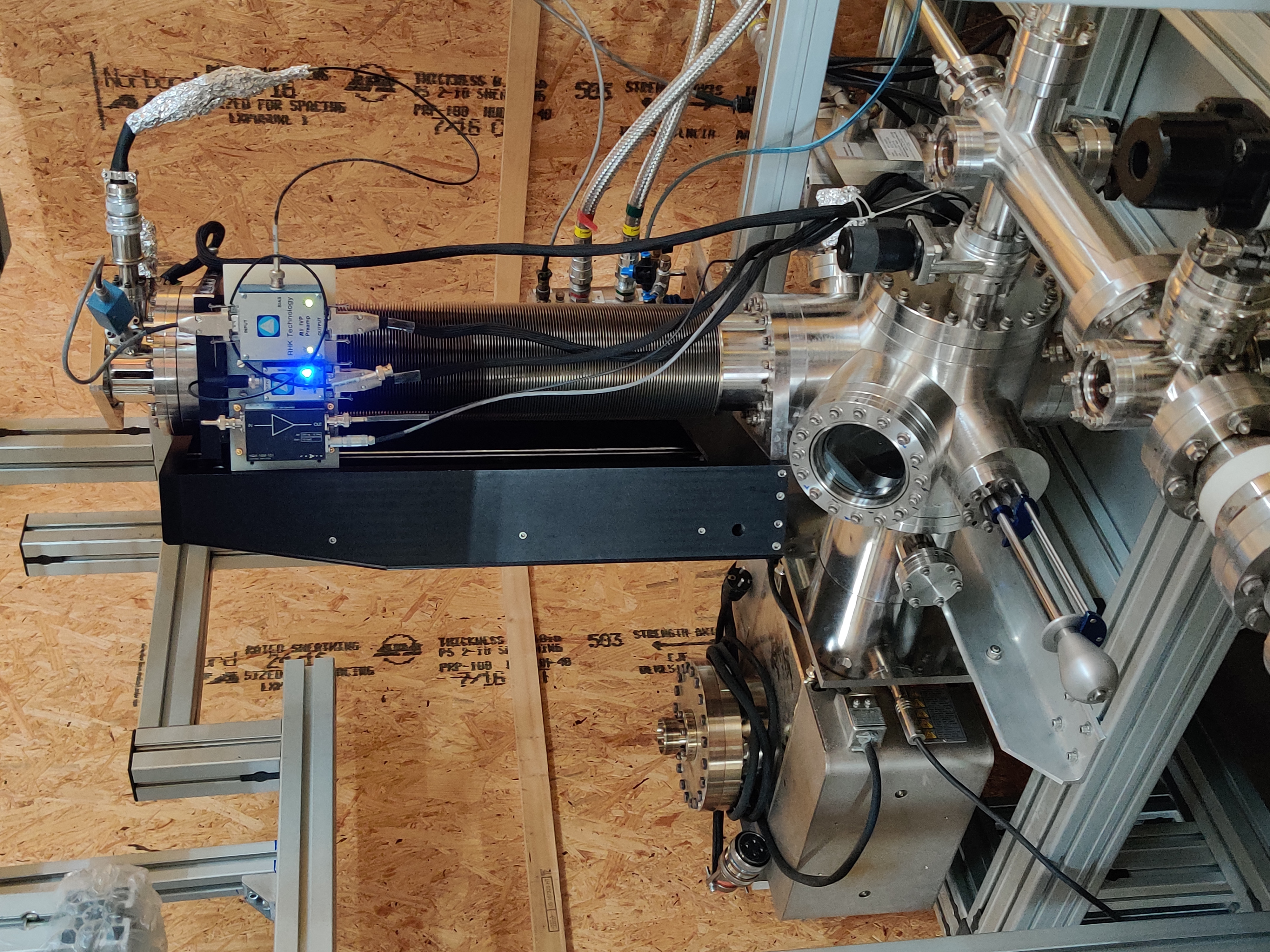
Scanning Tunneling Microscope (LT-STM)
Our lab houses the world’s first cryogen-free STM with a cryogen-free magnet capable of vertical fields up to 5 T and in-plane fields up to 1 T.
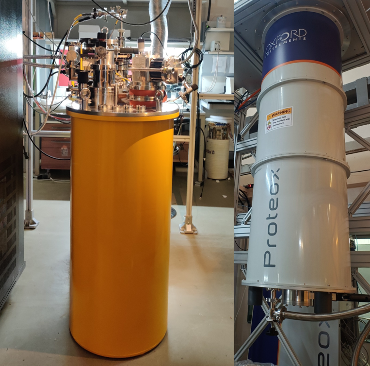
Cryogenic Systems
The VTI cryostat and Dilution Refrigerator enable magnetotransport measurements down to 1.5 K, with the VTI Cryostat offering a 9 T field for low-temperature experiments.
Access to TIFR Shared Facilities
We also benefit from access to world-class shared facilities at TIFR Hyderabad, including:
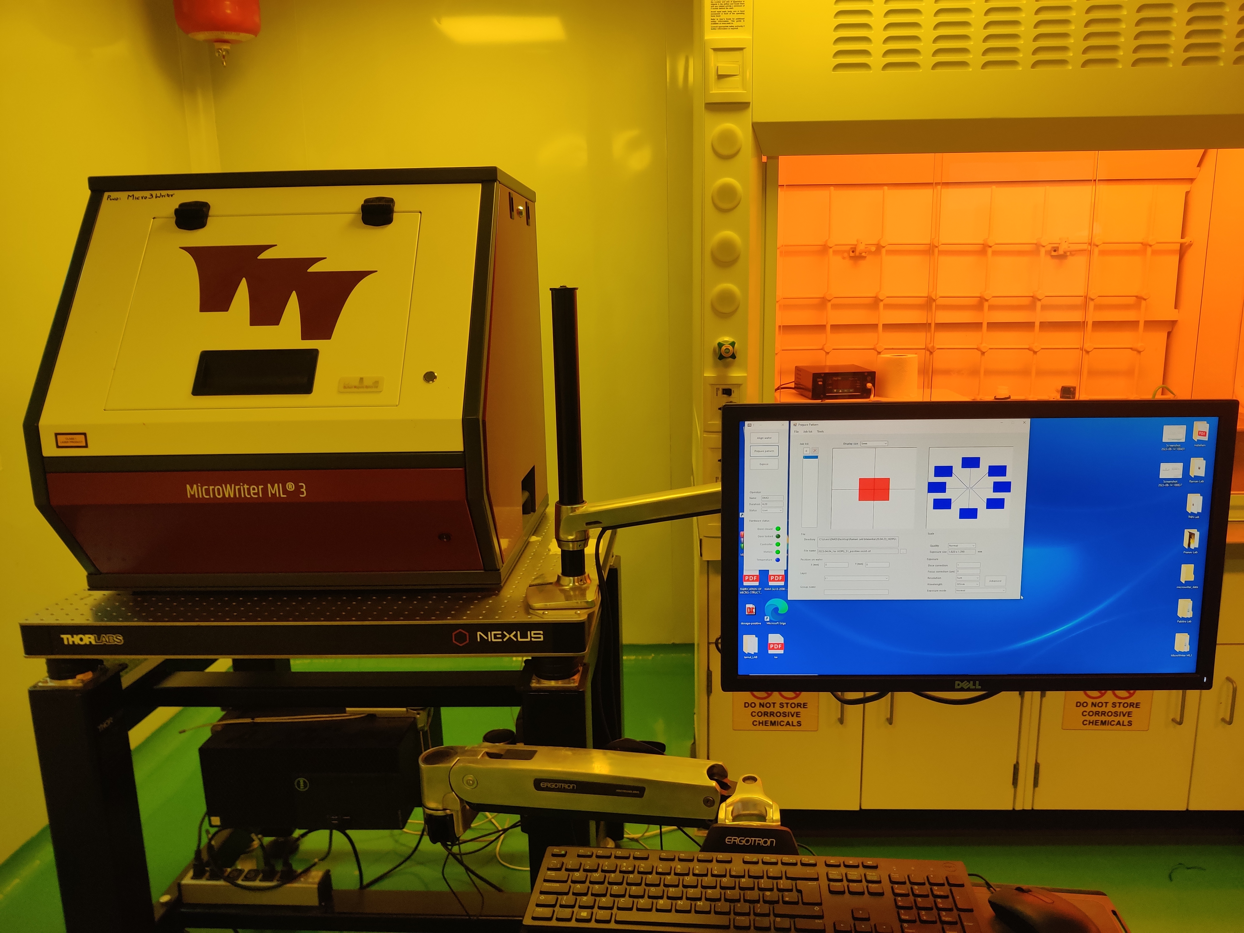
- Cleanroom Facility: State-of-the-art cleanroom for laser writer lithography, maskless patterning, soft lithography, and SEM with E-beam lithography.
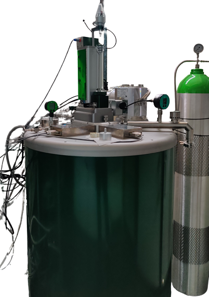
- Superconducting Quantum Interference Device (SQUID)
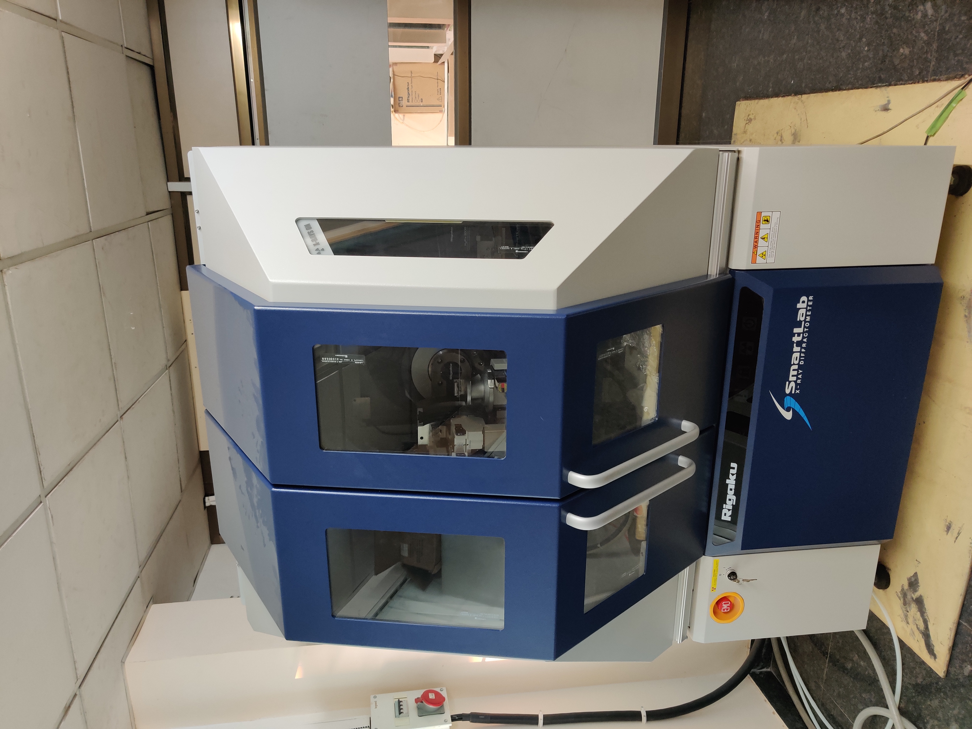
- X-ray Diffractometer
Opportunities
The Raman Lab is always looking for motivated and talented individuals to join our team. We offer a dynamic and collaborative research environment at the forefront of condensed matter physics.
Available Positions:
- Junior Research Fellows (JRFs) & Interns
- PhD Students (Integrated PhD & Regular PhD)
- Postdoctoral Fellows
- Visiting Scientists
Prospective candidates are encouraged to send their CV and a brief statement of research interests to the Principal Investigator. Please check the TIFR Hyderabad website for official announcements and application procedures.
Contact
Principal Investigator:

Dr. Karthik V. Raman
Associate Professor
Tata Institute of Fundamental Research (TIFR)
Hyderabad, India
Email: kvraman@tifrh.res.in
Phone: +91-40-2020-XXXX (TIFR Main)

